Teachers' Domain - Digital Media for the Classroom and Professional Development
User: Preview

Source: Pennsylvania College of Technology/WVIA
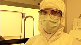
In this video segment adapted from Pennsylvania College of Technology and WVIA, learn about nanotechnology and nanofabrication. Meet Mark Atwater, a student enrolled in a nanotechnology program, who takes you on a tour of a nanofabrication lab. Observe the "bunny suit" he needs to wear to prevent contamination of the lab, and learn about the top-down fabrication process of photolithography. In addition, Mark discusses his goals for the future and why this experience is so valuable.
It is likely that advances in nanotechnology—the technology of extremely small things—will affect the way that almost everything is made in the future. A nanometer is just one billionth of a meter (approximately the width of a few atoms); nanotechnology has enabled the ability to manipulate matter at the molecular scale for practical uses in a wide range of applications, from sports equipment to pharmaceuticals. This diverse and exciting field is growing rapidly and creating a revolution in manufacturing. For students seeking careers in a dynamic and cutting-edge industry, nanotechnology seems to offer endless opportunities.
But how are nanomaterials made? Nanoscale devices are typically less than 100 nanometers in size. The process of engineering such tiny structures requires special techniques and an exceptionally clean environment free of contaminants. The critical dimension, or size, of nanostructures is so small that a single speck of hair or dust would destroy the product.
There are two fundamentally different methods for fabricating nanostructures: top-down and bottom-up. One approach is like carving a sculpture out of a large block of stone (material is removed to produce a new product), and the other approach is like building a stone wall (material is added to produce a new product).
Top-down nanofabrication produces nanosized structures by carving down larger materials. One example of this process is photolithography, which uses light to transfer an image onto a surface. The surface is covered with a light-sensitive chemical, called photoresist, which reacts when exposed to light. By projecting light through a mask, or stencil, the pattern on the mask is transferred into the photoresist. Once exposed, the photoresist is developed and the desired pattern is left behind. The pattern is later transferred to the layer beneath the photoresist using an etch process. Nano-sized features can be made using this technique by scaling down the image with the aid of optics. For example, patterns of very thin lines can be created on a surface to make networks of tiny wires. Computer chip manufacturing and microsystems fabrication utilize similar processes.
In contrast, bottom-up nanofabrication produces nanomaterials by building up structures atom by atom, molecule by molecule. Using their chemical properties, atoms and molecules are assembled into larger structures. This approach is based on the self-assembly process found in nature (seen, for example, in the formation of crystals and biological molecules). Soap bubbles demonstrate one such process that is used for nanofabrication: the self-assembly of monolayers (layers of molecules one molecule thick). When soap molecules interact with water, they naturally assemble into two single layers, or monolayers, of molecules because they have one end that is attracted to water and one that is not. Bottom-up fabrication has an advantage over top-down fabrication in that it does not waste material and allows for smaller geometries, but it is not as well established. However, as the field of nanotechnology progresses, bottom-up fabrication techniques will advance and become more prevalent.
 Loading Standards
 Teachers' Domain is proud to be a Pathways portal to the National Science Digital Library.
